Think of pharmaceutical companies as less to do with pharmaceuticals and a lot more to do with delivery systems. The more delivery systems you have, the easier it is to hide and stealth the delivery. For example, instead of the logical thing and picking out the best pharmaceutical company with the best product to introduce to the fake pandemic, they introduce an entire slew of pharmaceutical companies into the fray all at once, all under the clever pretense of equal competition, of course. This allows them to have a plethora of different delivery systems, while offering them many stealth and obfuscation opportunities. Like finding a needle in a haystack.
GRAPHINE

Despite the promising results in different cell studies and proof of concept studies, there is still incomplete understanding of the full biocompatibility of graphene based materials.[181] Different cell lines react differently when exposed to graphene, and it has been shown that the lateral size of the graphene flakes, the form and surface chemistry can elicit different biological responses on the same cell line.[182]
There are indications that Graphene has promise as a useful material for interacting with neural cells; studies on cultured neural cells show limited success.[183][184]
Graphene also has some utility in osteogenics. Researchers at the Graphene Research Centre at the National University of Singapore (NUS) discovered in 2011 the ability of graphene to accelerate the osteogenic differentiation of human Mesenchymal Stem Cells without the use of biochemical inducers.[185]
Graphene can be used in biosensors; in 2015 researchers demonstrated that a graphene-based sensor be can used to detect a cancer risk biomarker. In particular, by using epitaxial graphene on silicon carbide, they were repeatably able to detect 8-hydroxydeoxyguanosine (8-OHdG), a DNA damage biomarker.[186]
Support substrate
The electronics property of graphene can be significantly influenced by the supporting substrate. Studies of graphene monolayers on clean and hydrogen(H)-passivated silicon (100) (Si(100)/H) surfaces have been performed.[187] The Si(100)/H surface does not perturb the electronic properties of graphene, whereas the interaction between the clean Si(100) surface and graphene changes the electronic states of graphene significantly. This effect results from the covalent bonding between C and surface Si atoms, modifying the π-orbital network of the graphene layer. The local density of states shows that the bonded C and Si surface states are highly disturbed near the Fermi energy.
Bilayer graphene displays the anomalous quantum Hall effect, a tunable band gap[191] and potential for excitonic condensation[192] –making it a promising candidate for optoelectronic and nanoelectronic applications. Bilayer graphene typically can be found either in twisted configurations where the two layers are rotated relative to each other or graphitic Bernal stacked configurations where half the atoms in one layer lie atop half the atoms in the other.[193] Stacking order and orientation govern the optical and electronic properties of bilayer graphene.
One way to synthesize bilayer graphene is via chemical vapor deposition, which can produce large bilayer regions that almost exclusively conform to a Bernal stack geometry.[193]
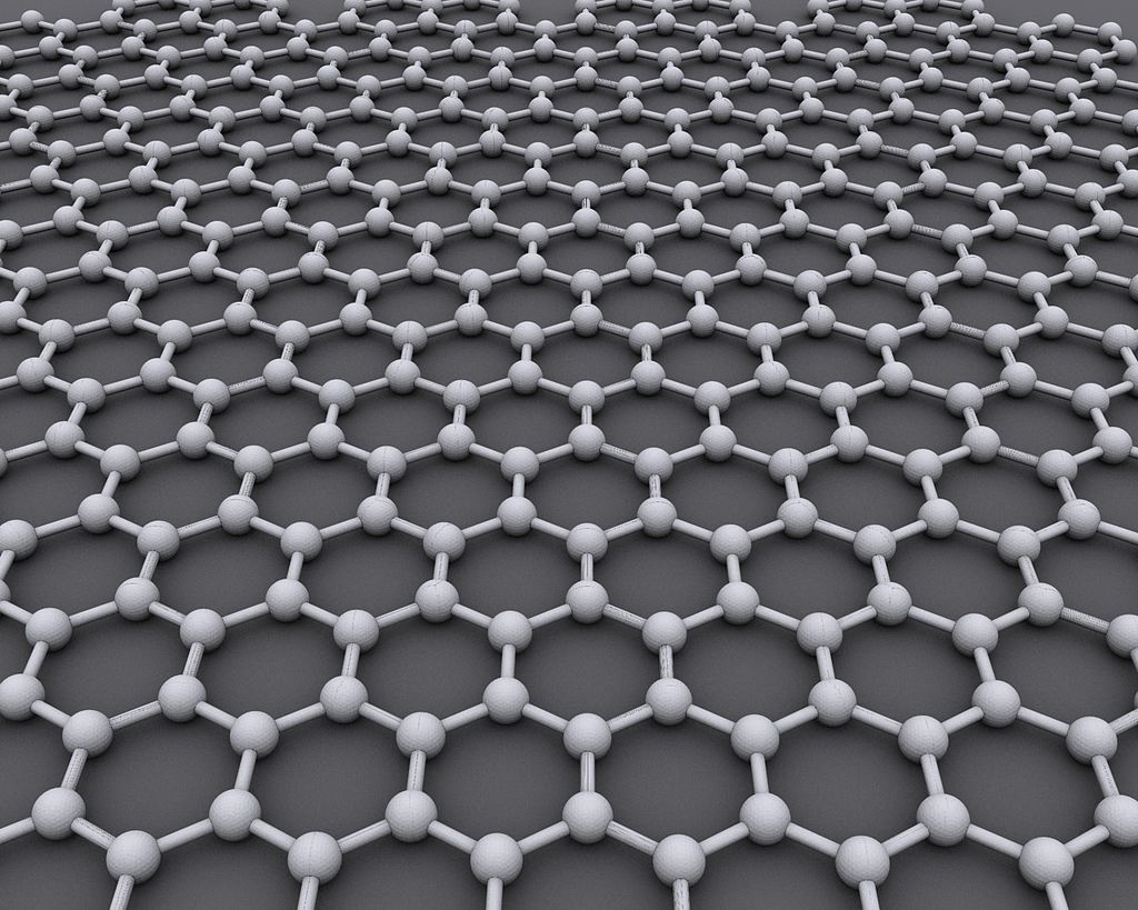
Graphene (/ˈɡræfiːn/[1]) is an allotrope of carbon consisting of a single layer of atoms arranged in a two-dimensional honeycomb lattice[2][3] nanostructure.[4] The name is derived from "graphite" and the suffix -ene, reflecting the fact that the graphite allotrope of carbon contains numerous double bonds.
Each atom in a graphene sheet is connected to its three nearest neighbors by a σ-bond, and contributes one electron to a conduction band that extends over the whole sheet. This is the same type of bonding seen in carbon nanotubes and polycyclic aromatic hydrocarbons, and (partially) in fullerenes and glassy carbon.[5][6] These conduction bands make graphene a semimetal with unusual electronic properties that are best described by theories for massless relativistic particles.[2] Charge carriers in graphene show linear, rather than quadratic, dependence of energy on momentum, and field-effect transistors with graphene can be made that show bipolar conduction. Charge transport is ballistic over long distances; the material exhibits large quantum oscillations and large and nonlinear diamagnetism.[7] Graphene conducts heat and electricity very efficiently along its plane. The material strongly absorbs light of all visible wavelengths,[8][9] which accounts for the black color of graphite; yet a single graphene sheet is nearly transparent because of its extreme thinness. The material is also about 100 times stronger than would be the strongest steel of the same thickness.[10][11]
Graphene has become valuable and useful nanomaterial due to its exceptionally high tensile strength, electrical conductivity, transparency, and being the thinnest two-dimensional material in the world.[4] The global market for graphene was $9 million in 2012,[15] with most of the demand from research and development in semiconductor, electronics, electric batteries,[16] and composites.


